

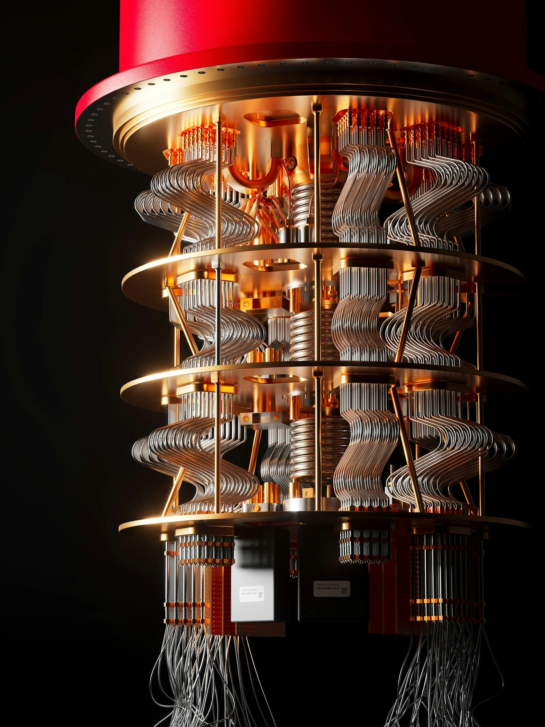
DEFENSE. COMPUTING. SPACE.
Superconductors have physics-based advantages over semiconductors for many sensing and computing applications. Ambature offers a versatile technology platform to bridge quantum and classical worlds.
THE BIG PICTURES

QUANTUM SENSORS
Defending the free world requires deploying the most sensitive detectors humans have ever made.
Improving patient outcomes requires clearer, timely imaging.
Autonomous vehicles need to know where everything is.

HIGH-PERFORMANCE COMPUTING
Solving the AI energy problem requires building the fastest and most efficient data centers.
Combining quantum computers and classical computers will optimize problem-solving.
The transition to superconductors is the biggest shift in the semiconductor industry since silicon.

NEW MATERIALS
Unlocking fusion energy requires the world’s strongest magnets.
Energy-intensive applications like data centers are increasingly building their own microgrids.
Higher-temperature superconductors unlock more deployments, and room-temperature superconductors are a holy grail of the materials and energy industries.

APPLICATIONS
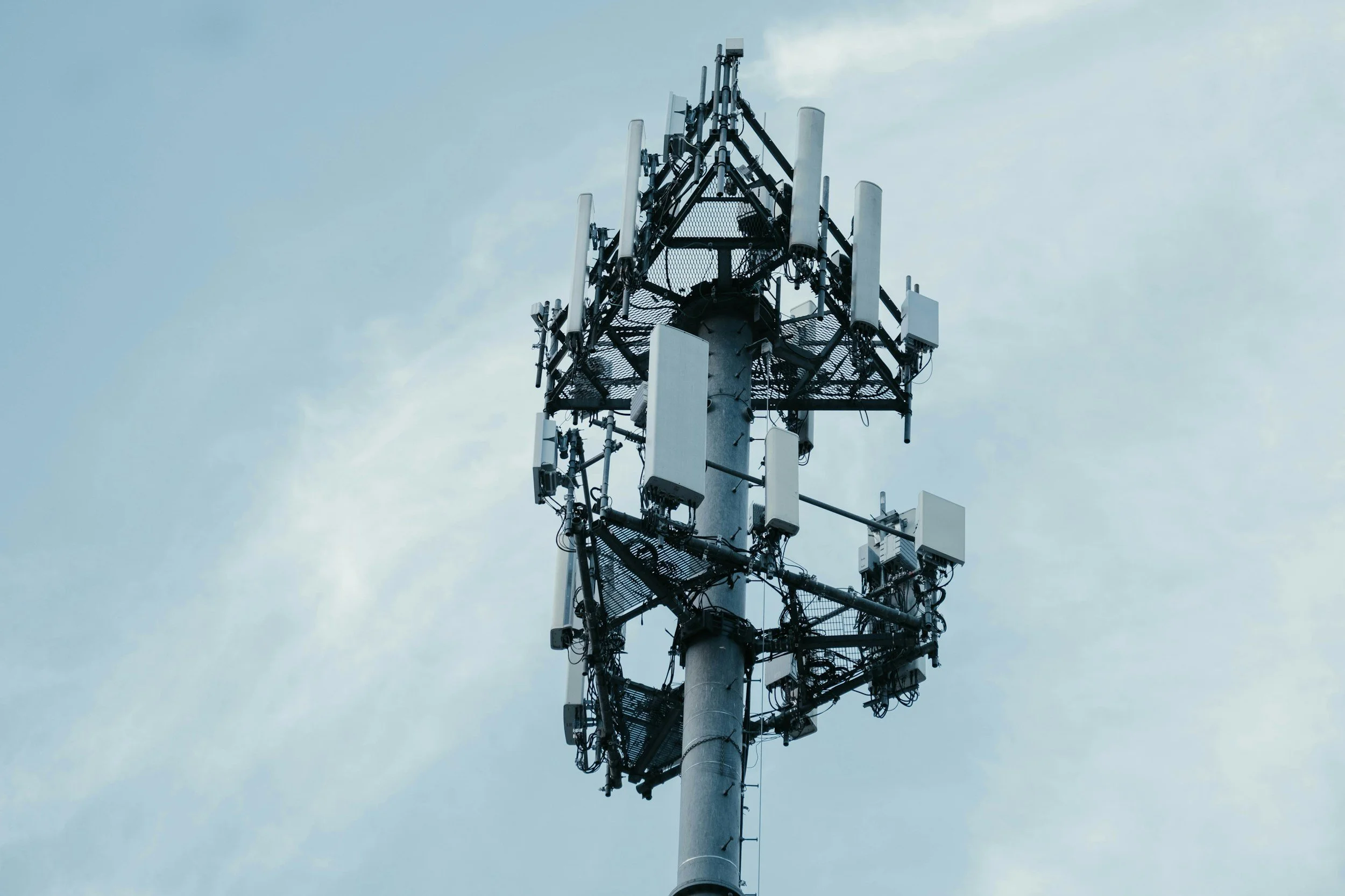
RF RECEIVERS
SQUID array sensors can be configured to cover a large range of frequencies from ELF to SHF.
One receiver can replace multiple traditional antennas for efficient procurement, logistics, and maintenance.
Superconductors enable small receivers even for very low frequencies while offering broader bandwidth than traditional electrically small antennas.
Cell phone towers can combine superconducting receivers with superconducting miniaturized data centers for the ability to process enormous amounts of data at the edge.
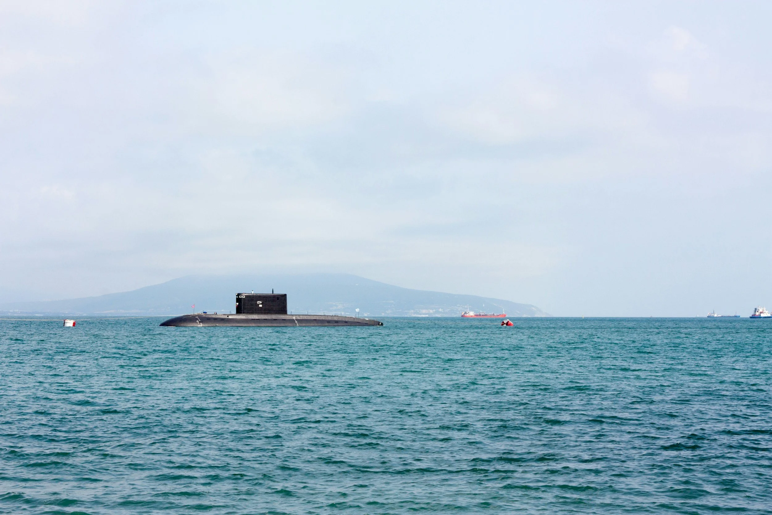
MAGNETIC ANOMALY DETECTORS
SQUID magnetometers, gradiometers, and gravimeters can detect threats like enemy vessels and unexploded ordnance (UXO).

MAGNETIC NAVIGATION
Magnetic navigation can supplement inertial navigation systems and provide an unjammable alternative to GPS/GNSS.
RADAR
Radar is in a continual arms race to see further while being less detectable.
Early warning networks are crucial for NORAD, the Golden Dome, and defending the arctic.
SQUIDs can enable greater range for radar warning receivers and low-probability-of-intercept radar with their exceptional sensitivity.
NONDESTRUCTIVE EVALUATION
SQUIDs can very accurately detect corrosion and deep cracks in aircraft components and other parts.
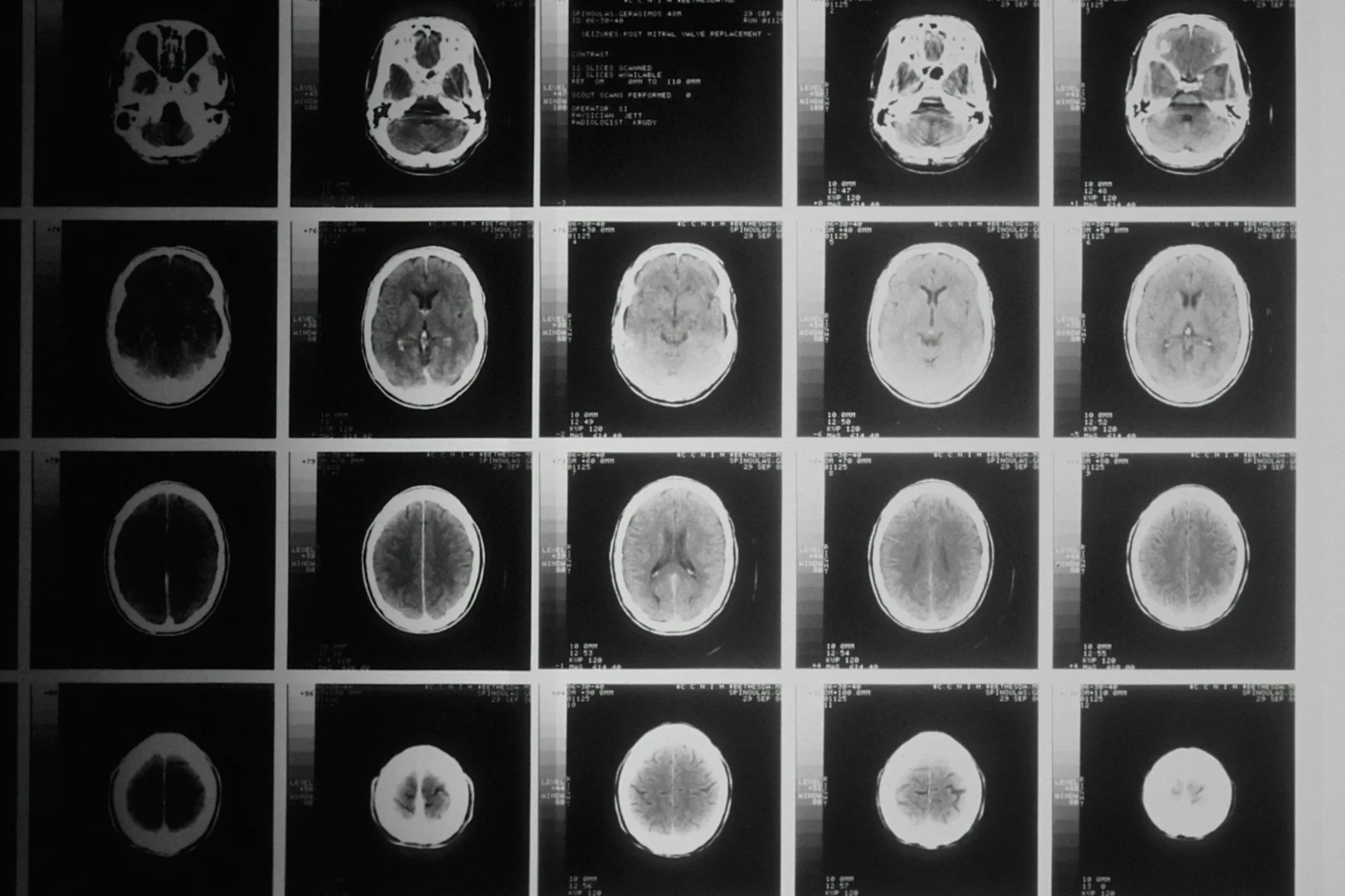
DIAGNOSTIC MEDICAL IMAGING
SQUIDs can produce clearer images than the conventional detectors used in MRI, MEG, and MCG.
They can enable portable and point-of-care imaging devices.
Small diagnostic devices based on smaller magnet fields can eliminate much of the ionized radiation modalities such as X-ray, CT, and PET. A small ultrasound device can be used for most other imaging.
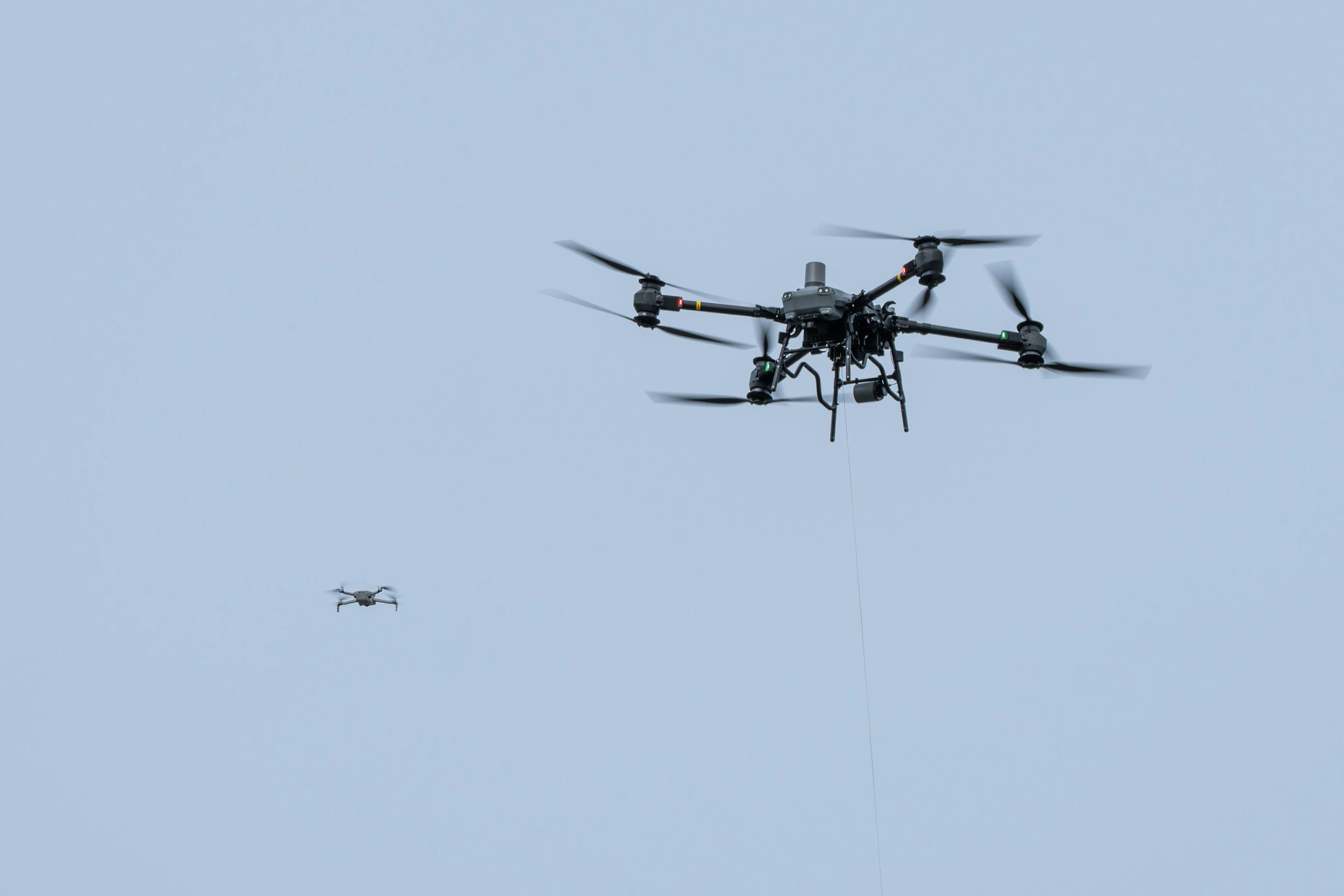
DRONES, EDGE SENSORS & EDGE COMPUTE
Superconducting sensing and computing modules can be combined and optimized for different SWaP scenarios, enabling distributed, highly-capable assets. Mid-sized aerial, surface, and underwater drones can field superconducting communications, threat detection, and processing functions using one small cryocooler.
IOT & SMART CITY INFRASTRUCTURE
SQUIDs can precisely detect the electromagnetic fields important to the operation of autonomous vehicles, industrial equipment, and smart city infrastructure, where synergies exist with HTS clean energy applications such as magnets, cable systems, fault current limiters, transformers, and energy storage / load balancing systems.

PHOTON DETECTORS
Superconductors can be used to implement superconducting nanowire single photon detectors (SNSPDs) and transition-edge sensors (TES) for quantum computing, night vision, and other applications.

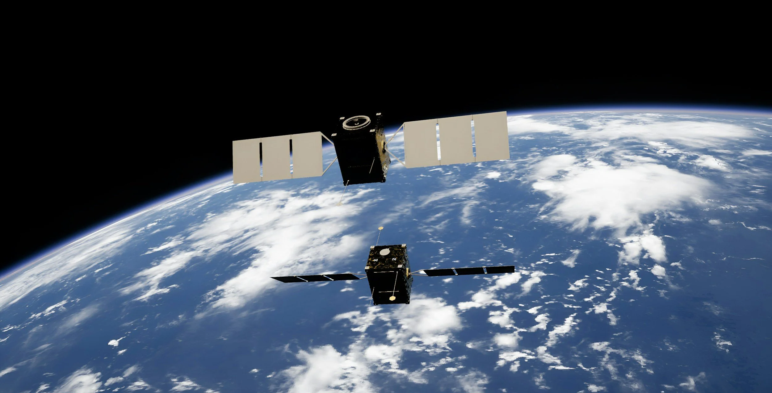
SPACE
The operating temperatures, high sensitivity, low heat dissipation, and dense compute system architectures make HTS satellites a natural way to scale infrastructure in space. With global attention and efforts to deploy space systems, HTS technologies enable smaller, more capable satellites that are easier to launch.
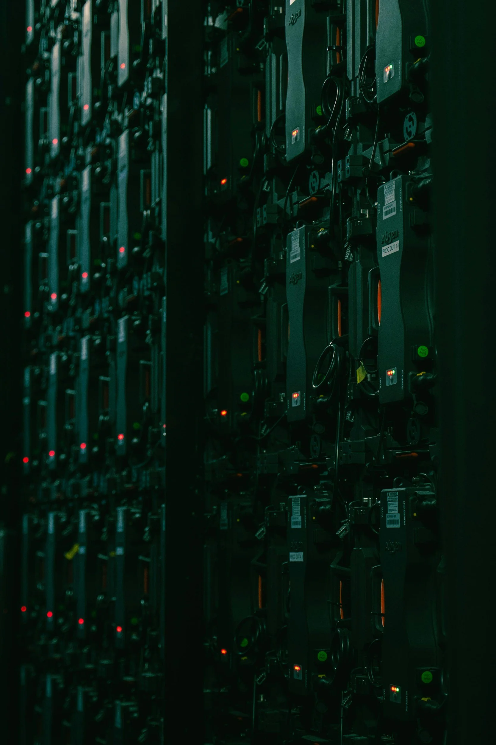
CLASSICAL COMPUTING
HTS supercomputers and data centers can be orders-of-magnitude more energy-efficient than semiconductor counterparts.
They will take up far less space because superconducting chips do not dissipate heat like semiconductor chips do, so they can be stacked in close proximity without overheating.
Superconducting chips can also run faster than semiconductor chips. Hybrid semiconductor-superconductor chips can also run faster because superconducting interconnects are far less resistant than copper interconnects, so RC delays can be minimized.
QUANTUM COMPUTING
Superconducting qubits are among the primary methods to create quantum computers (superconducting, photonic, neutral atoms, trapped ions, and others). While HTS are unlikely to be used to implement qubits in the near term due to the additional thermal noise inherent to operating at higher temperatures, HTS photon detectors, control circuits, and data processors can minimize room temperature system components/space. HTS photon detectors in particular can be used across multiple qubit types because even the room temperature" qubit systems often have cryogenic components.
The nation that leads in quantum sensing technology will gain decisive advantages in navigation, communications, resource exploration, and national defense.
The nation that leads in quantum sensing technology will gain decisive advantages in navigation, communications, resource exploration, and national defense.
Vivek Lall & Haibo Huang, General Atomics for the Hoover Institution
WHY NOW
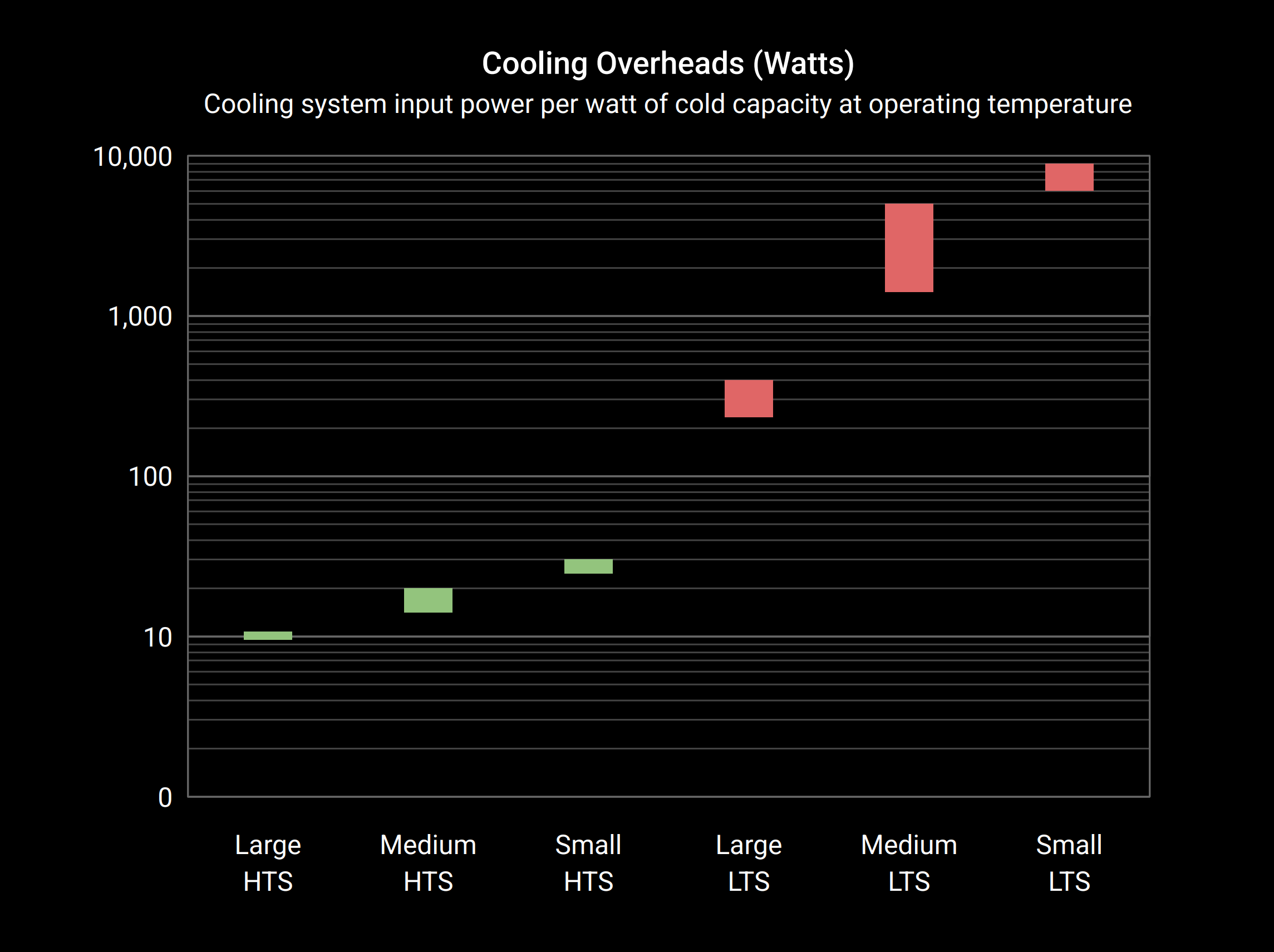
Adoption of superconducting technologies has been limited by operational cooling requirements associated with low-temperature superconductors (LTS) and complex fabrication processes associated with high-temperature superconductors (HTS). Ambature’s uniquely-oriented “a-axis” HTS materials, devices, and processes offer the best of both worlds, enabling commercial-scale adoption of superconducting technologies for the first time. At the same time, major powers are in a quantum arms race, HPC/AI proliferation is hitting energy bottlenecks, and the semiconductor industry is exploring new materials and architectures to continue performance scaling as semiconductors approach fundamental limits.
JOSEPHSON JUNCTIONS
JJs are the fundamental building blocks of superconducting circuits. They’re superconducting counterparts to semiconductor transistors.
JJs in parallel make superconducting quantum interference devices (SQUIDs), which can implement the most sensitive magnetic sensors humans have ever made. They are key components in a wide variety of sensing applications as well as quantum computing.
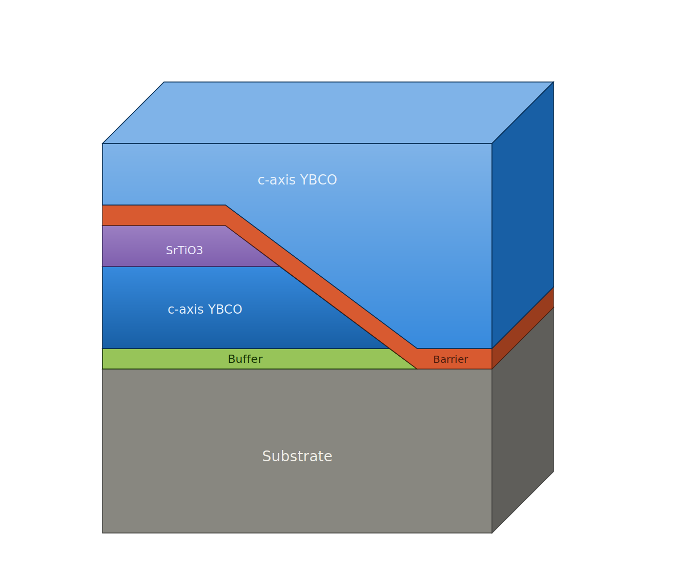
LTS VERTICAL TRILAYER
This is the industry standard architecture used to make superconducting qubits for quantum computing. Those who have access to this architecture use it exclusively.
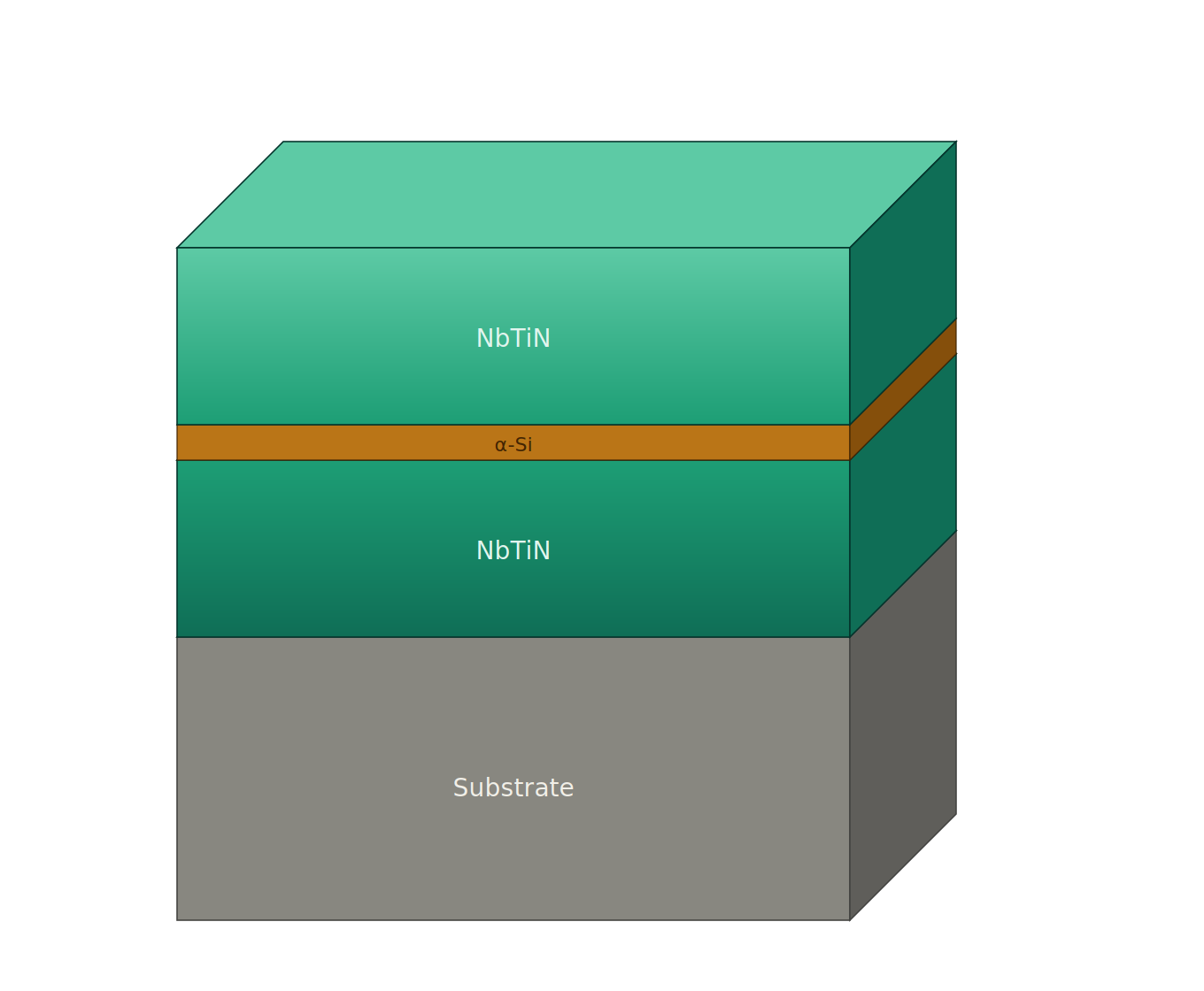
HTS HORIZONTAL
Conventional ramp-edge, step-edge, and other JJs evolved at a time when HTS vertical trilayer JJs were not available. They are notoriously difficult to manufacture uniformly.
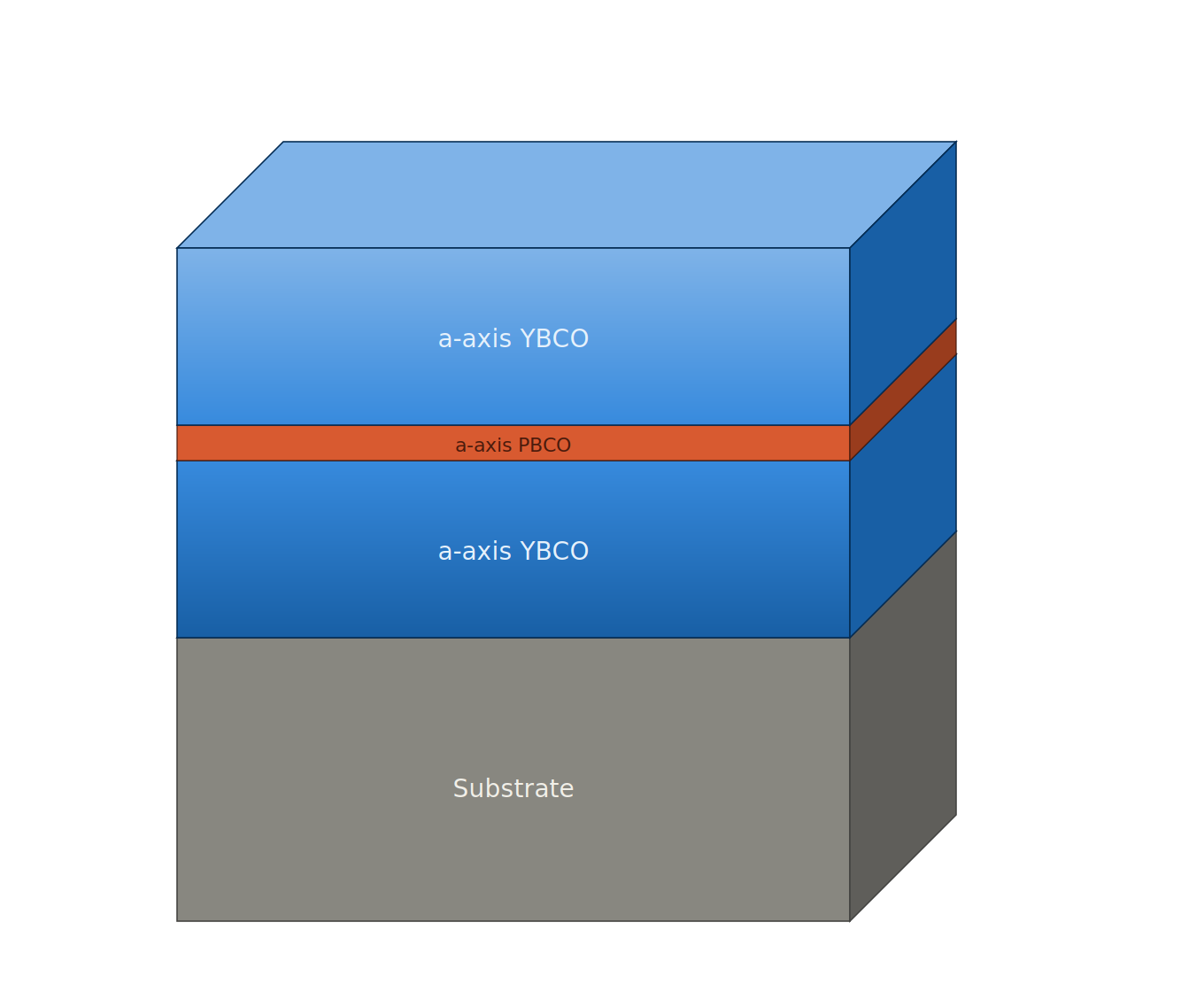
HTS VERTICAL TRILAYER
Ambature’s breakthrough a-axis epitaxy makes the industry standard architecture available in HTS for the first time, enabling scalable manufacturing of HTS microelectronics in semiconductor fabs.
The nation that best seizes the superconducting digital circuit opportunity will enjoy computing superiority for decades to come.
The nation that best seizes the superconducting digital circuit opportunity will enjoy computing superiority for decades to come.
Ivan Sutherland, CMOS Pioneer for the New York Times
intellectual property
Ambature has one of the largest patent portfolios pertaining to high-temperature superconductors in the world, with more than 3,800 unique claims issued in multiple major jurisdictions around the world. Our patents have been cited in more than 400 third-party patent applications, and we have an exceptional international network of partners commercializing our technology.
Apple
〰️
Brookhaven
〰️
D-Wave
〰️
GE
〰️
〰️
Halliburton
〰️
Hitachi
〰️
HRL Laboratories
〰️
Huawei
〰️
Hypres
〰️
IBM
〰️
Toshiba
〰️
MIT
〰️
Microchip Technology
〰️
Microsoft
〰️
PsiQuantum
〰️
Samsung
〰️
Seagate
〰️
SEEQC
〰️
Siemens
〰️
Tokamak Energy
〰️
Waymo
〰️
Apple 〰️ Brookhaven 〰️ D-Wave 〰️ GE 〰️ Google 〰️ Halliburton 〰️ Hitachi 〰️ HRL Laboratories 〰️ Huawei 〰️ Hypres 〰️ IBM 〰️ Toshiba 〰️ MIT 〰️ Microchip Technology 〰️ Microsoft 〰️ PsiQuantum 〰️ Samsung 〰️ Seagate 〰️ SEEQC 〰️ Siemens 〰️ Tokamak Energy 〰️ Waymo 〰️
Dell
〰️
Université de Sherbrooke
〰️
University of Texas at Austin
〰️
Dalhousie University
〰️
The MITRE Corporation
〰️
Government of Canada
〰️
U.S. Government
〰️
Calian
〰️
Northrop Grumman
〰️
Lockheed Martin
〰️
RTX
〰️
L3Harris
〰️
MDA Space
〰️
UCLA CHIPS
〰️
University of Arizona
〰️
CGI
〰️
KAUST
〰️
ASU
〰️
NASA JPL
〰️
Cornell University
〰️
McMaster University
〰️
Dell 〰️ Université de Sherbrooke 〰️ University of Texas at Austin 〰️ Dalhousie University 〰️ The MITRE Corporation 〰️ Government of Canada 〰️ U.S. Government 〰️ Calian 〰️ Northrop Grumman 〰️ Lockheed Martin 〰️ RTX 〰️ L3Harris 〰️ MDA Space 〰️ UCLA CHIPS 〰️ University of Arizona 〰️ CGI 〰️ KAUST 〰️ ASU 〰️ NASA JPL 〰️ Cornell University 〰️ McMaster University 〰️
Our Team

Ron Kelly
CEO
Mitch Robson
CTO
Kaushik Kudtarkar
Scientist


Priyanka Brojabasi
Senior Scientist
Archana Tiwari
Senior Scientist

Sujatha Vijayakrishnan
Scientist
Akinwumi Akinpelu
Scientist
Michael Lebby
Science Advisor
Bill Langer
Board Chairman


Bruce Barnhill
Board Member
Michael Strasser
Board Member

Patrick Murphy
Board Member
Hemant Patel
Board Member

Anna Leese
Board Member
Raj Jammy
Board Member


Christopher Coates
Board Member
Catherine Blewett
Board Member
Rick Toering
Outside Legal
Alonzo Kelly
Advisor
Adam Kablanian
Advisor
Geoff Williamson
Advisor

Craig Changstrom
Advisor
Ron Stritch
Advisor

Davis Hartman
In Memoriam
Liam Kelly
Head of Development
Peter Kastelic
CFO
OPEN POSITIONS
-
Ambature is seeking a highly skilled fabrication scientist to support the development and fabrication of next-generation superconducting devices. This role centers on cleanroom microfabrication, thin-film processing, and electrical testing, with the goal of maturing Ambature’s high-temperature superconducting technologies into robust, repeatable, and scalable processes.
This is a hands-on cleanroom position based in Waterloo, Ontario working in the QNFCF, the University of Waterloo’s 8,000 sq ft nanofabrication facility, and its satellite labs. You will collaborate closely with Ambature’s Science Team to scale our R&D-level process into robust manufacturable workflows while improving yield, increasing throughput, and accelerating prototype development.
In this role, you will:
Own Ambature’s multi-step fabrication process end-to-end and serve as the internal and external subject-matter expert
Develop, optimize, and execute cleanroom fabrication processes for superconducting devices (e.g., Josephson junctions, SQUIDs)
Drive new process innovations by exploring novel materials, architectures, and fabrication approaches to push device performance and manufacturability forward
Perform thin-film deposition (PVD), photolithography, etching, and metrology in an ISO 5-7 cleanroom environment
Implement process controls, documentation, and continuous improvement methodologies to enhance reproducibility and yield of target KPIs
Apply structured, data-driven engineering methods to diagnose issues and optimize processes
Collaborate with Ambature’s Science Team to translate device designs into process flows and provide fabrication-driven insights
Maintain detailed experimental records, analyze data, and communicate results clearly to technical and non-technical audiences
Support IP development through process documentation, invention disclosures, and technical contributions
Ensure safe operation of cleanroom tools and adherence to facility protocols
Required Qualifications:
PhD or M.Sc (with equivalent experience) in engineering physics, materials science, electrical engineering, nanotechnology, or a related field
3 - 5 years of post-graduate experience developing multi-step fabrication processes in a cleanroom environment
Proficiency with thin-film deposition, photolithography, and wet/dry etching
Proficiency with metrology tools such as SEM, AFM, and profilometry
Experience with device testing and electrical characterization (I-V, 4pt, contact resistance)
Strong proficiency with data-driven engineering methods (DoE, RCA, and SPC)
Strong data analysis skills and proficiency with scientific plotting/reporting tools
Excellent communication skills and the ability to work both independently and collaboratively
Strong attention to detail, time management, and process discipline
Must be eligible to work in Canada. Start date negotiable
Desired Qualifications:
Experience with superconducting materials or devices (e.g., ReBCO, Josephson junctions, SQUIDs)
Experience with EBL for nanofabrication of small-scale devices
Familiarity with cryogenic measurement systems (e.g., PPMS, dilution refrigerators, LHe/LN2 probes)
Patents, publications, or demonstrated contributions to fabrication-driven R&D
What We Offer:
This is a full-time position with a salary range of $125,000 - $150,000 CAD
Comprehensive benefits
Equity/stock options
4 weeks paid vacation
Opportunities for IP contribution and publications
How to Apply:
Please send your CV to mitch.robson@ambature.com with “Senior Scientist” in the subject line.
-
We’re always looking for talented people who share our passion for superconducting technologies to join our team! If you have experience working with superconducting materials, devices, or simulations, we’d love to hear from you.
Even if we don’t have a specific role posted here, we’re continually exploring opportunities to bring exceptional individuals onto our team, especially those with industry experience.
Desired Qualifications:
3+ years of industry experience working with superconductors
Experience with ReBCO or other high-temperature superconductors
Patents or high impact papers
Testing: Expertise in cryogenic and RT electrical measurements of superconducting materials, devices, and circuits
Fabrication: Expertise in principles and techniques of cleanroom device fabrication (e.g. Photolithography, PVD/PLD deposition, dry etching) as well as characterization (e.g. SEM, AFM, optical)
Simulation: Expertise in simulating superconducting materials, devices, or circuits
How to Apply:
Please send your CV to mitch.robson@ambature.com
AWAITING FIRST CONTACT
Product Development. Collaborative Research. Sponsored Research. Design Services. Licensing. Business Inquiries.