
A-Axis Versus C-Axis Materials
To understand the difference between a-axis and c-axis materials, it is important to understand two things:
Firstly, what differentiates one material from another? A material is defined by its crystallographic structure, or lattice. The positions of atoms relative to each other are fixed within the lattice, and the lattice repeats itself over and over to make up the material.
Secondly, how do we create materials? We commonly use thin film epitaxy, which is the process of growing thin films by depositing layers of materials on top of a crystalline substrate. When we refer to a-axis versus c-axis materials, we’re really referring to the orientation of epitaxial growth relative to the substrate. If the three-dimensional lattice is defined using a, b, and c axes, then a-axis growth would have the a-axis oriented perpendicular to the substrate, while c-axis growth would have the c-axis oriented perpendicular to the substrate. YBCO contains planes of copper atoms that illustrate this difference quite well:

YBCO Lattice. The crystal structure of YBCO. Rswarbrick, CC BY-SA 3.0, via Wikimedia Commons.

C-Axis Epitaxial Growth. Copper planes are like stacked sheets of paper.
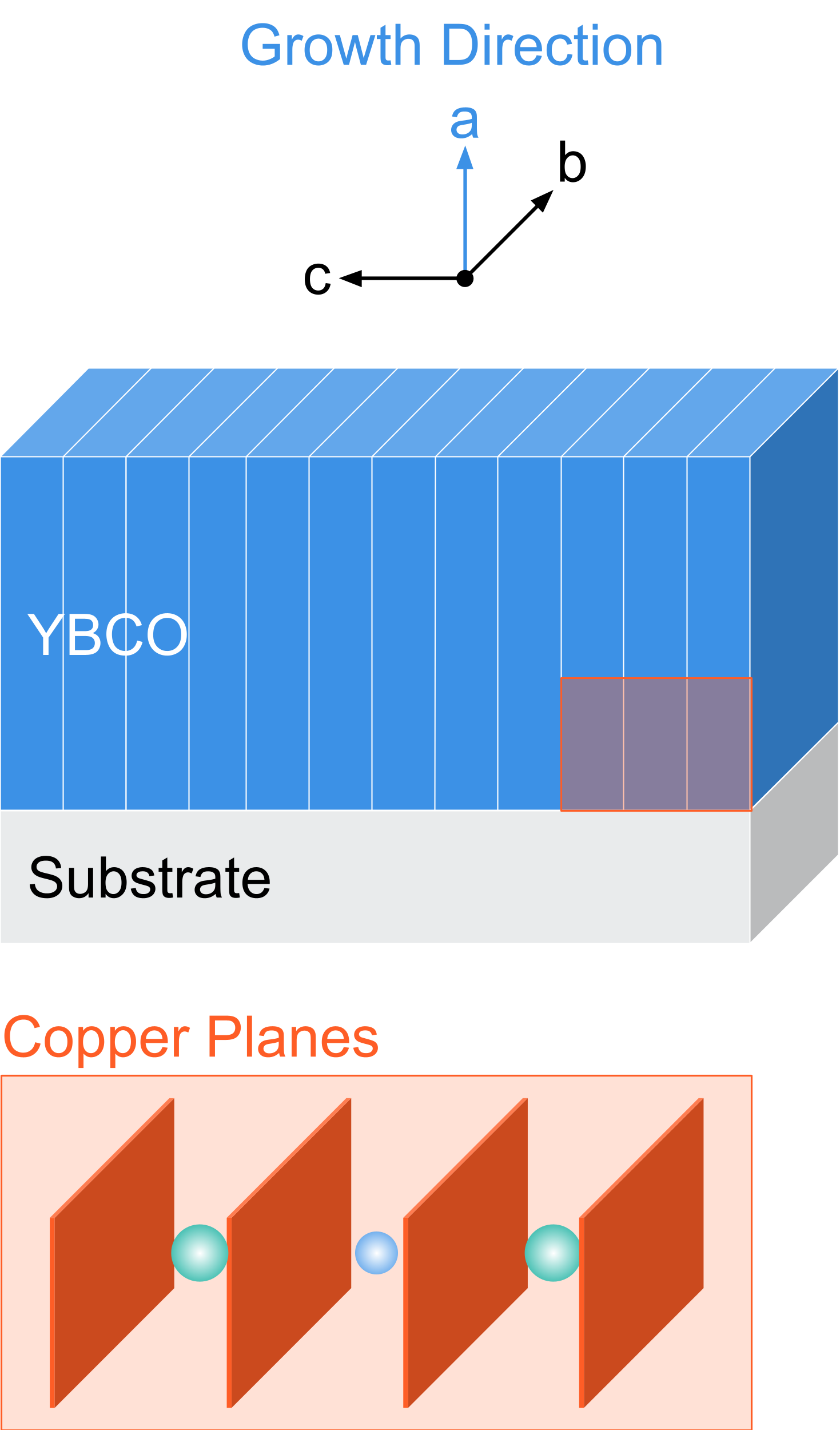
A-Axis Epitaxial Growth. Copper planes are like walls standing next to each other.
So, why would you prefer one orientation over the other? We’ll continue to explore the example of YBCO, but many considerations will be similar for the cuprates and other superconductors.
C-axis growth is easier. More technically, c-axis growth is kinematically favorable—nature prefers this configuration because it requires less work to accomplish. Superconducting materials like YBCO are conventionally grown along the c-axis for this reason.
Material properties may differ along the different axes. For example, superconducting coherence length is the average distance between the two electrons in a Cooper pair. Generally speaking, more stable superconducting states have longer coherence lengths. The copper planes in YBCO tend to impede superconductivity in the c direction. The resulting coherence lengths are 2 nanometers in the a direction, 2 nanometers in the b direction, and 0.2 to 0.4 nanometers (five to ten times smaller) in the c direction, so supercurrents prefer to flow in the a-b copper planes. This fundamental preference gives a-axis devices an inherent architectural advantage over c-axis devices: currents flow horizontally (parallel to the substrate) in c-axis materials, but currents can flow horizontally and vertically (parallel and perpendicular to the substrate) in a-axis materials.
This means a-axis devices are easier to fabricate, and they unlock new device and circuit architectures. Josephson junctions are great examples for this discussion. Josephson junctions are fundamental components of many superconducting electronics like sensors, quantum computers, and energy-efficient classical computers. Notice how much simpler an a-axis trilayer Josephson junction is when compared to a conventional c-axis junction:

Cross Section of A-Axis Trilayer Josephson Junction. This a-axis structure can be achieved in one continuous growth process on one machine.

Example Cross Section of C-Axis Ramp-Edge Josephson Junction. This c-axis structure requires three to five growth and etching processes on separate machines.
The simplicity, flexibility, and scalability of this a-axis design holds the potential for mass commercialization of superconducting electronics. We’ve dedicated an entire section to a-axis Josephson junctions if you’d like to learn more about them.