

What Are Superconductors?
You are probably familiar with semiconductors. After all, the computer, phone or tablet you’re reading this on is a semiconductor device. The “semi” in semiconductor means it conducts electricity with some resistance. You feel this resistance as your device heats up—energy is being lost. By contrast, a superconductor is any material that, under certain conditions, conducts electricity with no resistance—no loss. A supercurrent could go on forever. The caveat is that materials tend to transition to a superconducting state at very low temperatures, which have historically made them impractical for many applications, especially considering the impressive advancements and wide availability of semiconductors over the last many decades. Semiconductor progress is slowing, however, with nanometer processes nearing the physical limits of performance and energy-efficiency. Meanwhile, use cases are only becoming more demanding, with computing and sensing applications managing exponentially-increasing amounts of data. Industry needs new materials and new device architectures to exceed the boundaries of modern semiconductor paradigms. With superconductors reaching higher transition temperatures and cost-effective cooling solutions entering the market, superconducting devices are one clear solution to the problems the semiconductor industry faces. For our part, we believe Ambature’s a-axis materials and scalable device architectures will enable semiconductor companies to produce superconducting devices at industrial scale by simplifying fabrication, improving densities, and lowering cooling requirements when compared to traditional superconductors.
If you’d like to learn more about the history, properties and applications of superconductors, we recommend watching this video:
High-Temperature Superconductors
There are low-temperature superconductors (LTS) and high-temperature superconductors (HTS). HTS transition temperatures are still well below 0° Fahrenheit or Celsius, but researchers all over the world endeavor to create materials with higher transition temperatures because a room-temperature superconductor would be a Holy Grail of clean energy. Ambature’s roots are in HTS research, and many of our designs incorporate a-axis yttrium barium copper oxide (YBCO) and other members of the REBCO or cuprate family of superconductors. “Rare Earth” in REBCO is a misnomer—many of the elements are abundant in nature and widely used. You can find them in the electric motors of hybrid and electric vehicles, for example. Mining rare earth elements, much like mining any other resource, has limited environmental impact if safety standards and environmental regulations are followed, and rare earth recycling is increasing.
YBCO transitions at around 90 Kelvin (-298°F or -183°C), which means it can be cooled by liquid nitrogen. Liquid nitrogen is abundant, cost-effective, and used extensively in food processing and other industries, so there is a wealth of expertise in place to deal with liquid nitrogen at industrial scales. Real-world factors determine cooling performance, but we can use ideal calculations to explore potential gains. Cooling HTS to 77K with liquid nitrogen requires, ceteris paribus, about four percent of the power required to cool LTS to 4K with liquid helium. Increased noise at higher temperatures will not be suitable for all applications, but an optimal balance can be struck. Helium is also limited and more expensive than nitrogen. In our own lab activities, liquid helium costs more than 17 times as much as liquid nitrogen, including helium regeneration.
Ambature once produced an a-axis YBCO/NBCO superlattice that partially transitioned above 200K, prompting our national lab partners at the time, a division of NASA’s Jet Propulsion Laboratory, to publish that Ambature has “fabricated and tested a material that arguably holds promises for room temperature superconductivity.” A superlattice is a compound superconductor comprising many layers of superconducting materials. Each layer reinforces the stack to achieve a higher transition temperature. We are growing and testing new superlattices this quarter to further investigate the potential of a-axis HTS.

A-Axis Versus C-Axis Materials
To understand the difference between a-axis and c-axis materials, it is important to understand two things:
Firstly, what differentiates one material from another? A material is defined by its crystallographic structure, or lattice. The positions of atoms relative to each other are fixed within the lattice, and the lattice repeats itself over and over to make up the material.
Secondly, how do we create materials? We commonly use thin film epitaxy, which is the process of growing thin films by depositing layers of materials on top of a crystalline substrate. When we refer to a-axis versus c-axis materials, we’re really referring to the orientation of epitaxial growth relative to the substrate. If the three-dimensional lattice is defined using a, b, and c axes, then a-axis growth would have the a-axis oriented perpendicular to the substrate, while c-axis growth would have the c-axis oriented perpendicular to the substrate. YBCO contains planes of copper atoms that illustrate this difference quite well:

YBCO Lattice. The crystal structure of YBCO. Rswarbrick, CC BY-SA 3.0, via Wikimedia Commons.

C-Axis Epitaxial Growth. Copper planes are like stacked sheets of paper.
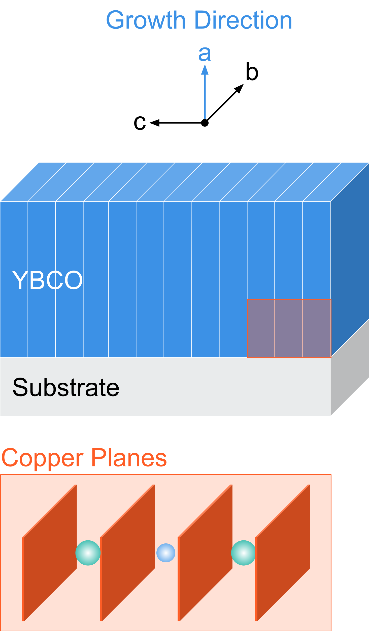
A-Axis Epitaxial Growth. Copper planes are like walls standing next to each other.
So, why would you prefer one orientation over the other? We’ll continue to explore the example of YBCO, but many considerations will be similar for the cuprates and other superconductors.
C-axis growth is easier. More technically, c-axis growth is kinematically favorable—nature prefers this configuration because it requires less work to accomplish. Superconducting materials like YBCO are conventionally grown along the c-axis for this reason.
Material properties may differ along the different axes. For example, superconducting coherence length is the average distance between the two electrons in a Cooper pair. Generally speaking, more stable superconducting states have longer coherence lengths. The copper planes in YBCO tend to impede superconductivity in the c direction. The resulting coherence lengths are 2 nanometers in the a direction, 2 nanometers in the b direction, and 0.2 to 0.4 nanometers (five to ten times smaller) in the c direction, so supercurrents prefer to flow in the a-b copper planes. This fundamental preference gives a-axis devices an inherent architectural advantage over c-axis devices: currents flow horizontally (parallel to the substrate) in c-axis materials, but currents can flow horizontally and vertically (parallel and perpendicular to the substrate) in a-axis materials.
This means a-axis devices are easier to fabricate, and they unlock new device and circuit architectures. Josephson junctions are great examples for this discussion. Josephson junctions are fundamental components of many superconducting electronics like sensors, quantum computers, and energy-efficient classical computers. Notice how much simpler an a-axis trilayer Josephson junction is when compared to a conventional c-axis junction:

Cross Section of A-Axis Trilayer Josephson Junction. This a-axis structure can be achieved in one continuous growth process on one machine.

Example Cross Section of C-Axis Ramp-Edge Josephson Junction. This c-axis structure requires three to five growth and etching processes on separate machines.
The simplicity, flexibility, and scalability of this a-axis design holds the potential for mass commercialization of superconducting electronics. We’ve dedicated an entire section to a-axis Josephson junctions if you’d like to learn more about them.
A-Axis Epitaxy
Recall that nature prefers c-axis growth; convincing copper planes to stand on their edges is kinematically challenging. For industry to take advantage of a-axis devices, someone had to overcome the challenges of a-axis growth.
It turned out that someone was Ambature. We hired Cornell University under a sponsored research contract to determine which growth conditions—such as temperature and pressure—are needed to convince nature that a-axis growth is kinematically and thermodynamically favorable. Ambature’s breakthrough epitaxial technology has been demonstrated to reproducibly grow high-quality thin film YBCO/PCBO layers along the a-axis with excellent smoothness and better than 97% a-axis purity. Cornell’s research paper was published in Applied Physics Letters, and our peer reviewers represented the Max Planck Society and Brookhaven National Laboratory.
Cornell Research Results. STEM-HAADF shows high-quality layers with near-perfect atomic alignment at interfaces. STEM-EELS shows precise control of layer composition.
“Samples obtain high quality, high superconducting transition temperature ~85 K, phase purity and improved surface quality with RMS roughness less than a-axis superconducting coherence length, making these films promising candidates for fabricating Josephson junctions and other electronic devices.” — Peer Reviewer from Max Planck Institute. “This is expected to be beneficial for fabrication of high-Tc Josephson junctions, a technologically very important and yet so far largely elusive target. This paper presents a significant step towards reaching this goal.” — Peer Reviewer from Brookhaven National Lab. You can read the Cornell paper on the American Institute of Physics website.
So, while the c-axis is easier from an epitaxial growth perspective, the a-axis is practical from fabrication and end-use perspectives. With Ambature’s proven ability to grow excellent a-axis materials, the choice is clear for semiconductor companies operating at industrial scale: a-axis devices are easier to make and use.